Inverse Design for Semiconductors
Research interest include Inverse Design: starting from the properties desired—such as, electronic bandgap, optical properties, carrier transport behavior, stability, defect tolerance—and working backwards to discover materials that satisfy the specification.
Instead of choosing a known compound and asking “what does it do?”, inverse design asks “what must the crystal be like to do this?” We use target metrics (e.g., bandgap, effective masses, dielectric response, phonon stability) as constraints and search the chemical + structural space top-down.
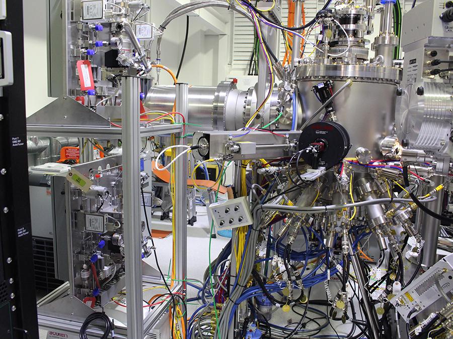
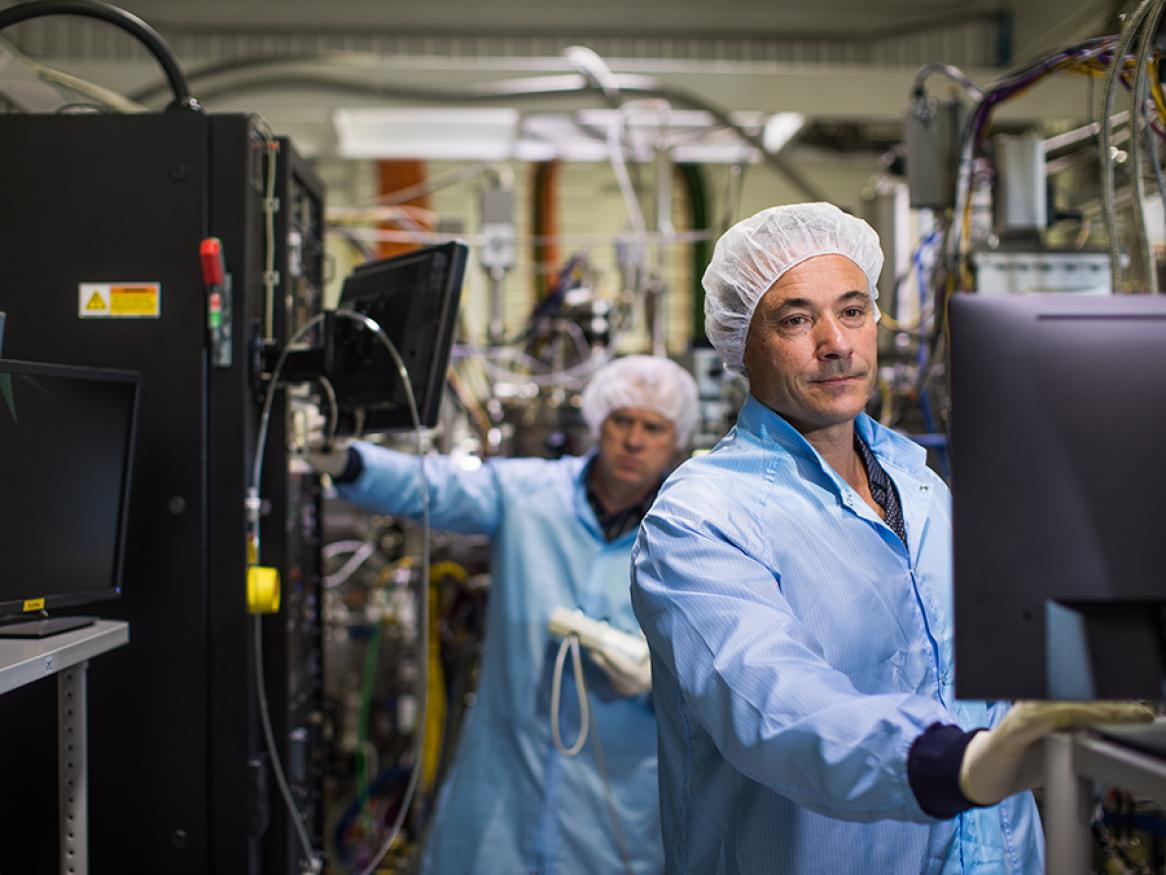
Promising candidates are then mapped into feasible crystal structures—space groups, Wyckoff positions, and bonding motifs—and screened for synthesizability. Finally, we make them real: grow or synthesize the material, measure its properties, and close the loop between prediction and experiment.
The goal is a pipeline from specification → structure → synthesis → validation.